Showing posts with label ATtiny. Show all posts

Friday, April 25, 2014

Wearable Electronics: Arduino X ATTiny85 with WS2812/2811 addressable RGB LED strip

Wearable Electronics: Arduino ISP ATTiny85 with WS2812/2811 addressable RGB LED strip
Many moons earlier, Mr.ChongSP ordered some individually addressable RGB LED strip (60LED/m) that uses WS2812 from middle country: aliexpress. Adafruit has a similar product, the Adafruit Neopixel. Yours truly manage to “BBS” 1x courtesy of Mr.ChongSP. Hardware is easy to procure, but “free” time to play with this new toy is hard to come by. Yours truly is working to the tune of “The Beatles-eight days a week” for the last couple of months. Nonetheless, when responsibility comes (to appear alongside Mr.JolyonC on stage for the Freshman Orientation Program “From Faraday to Fusion”), there is a need to push out the boat. The thing supposed to be a stage piece to grab freshie’s attention, so, addressable RGB LED on a jacket it shall be.

Since it is a wearable, there are several design (engineering) considerations. First, the Power supply unit, to power both the microcontroller (MCU) and the RGB LED Strip. Secondly, the size of the electronics package and thirdly, diffuser for RGB LED strip.
Using Arduino is a popular choice, given the footprint of it, it is easy to spot from a far. Not a good design choice. Furthermore, Arduino requires 9V supply whereas WS2812/2811 addressable RGB LED strip requires 5V. If both are used together, there is a need for a separate circuitry with both 7895 5v and 7809 9v voltage regulators, with supply being 12V 1A. Having said that, 12V battery pack and voltage regulator circuitry increase the footprint of the total package.
Therefore, the logical choice would be ATTiny85 that can be powered off from a 3to6V battery; PSU is a 5V 1A mobile power bank with USB connector that is meant for charging smart phones on the go. The choice of this PSU can be used to power both the addressable RGB strip and also ATTiny85.
As for the diffuser, 3D printed spikes using ninjaflex http://shin-ajaran.blogspot.sg/2014/04/3d-printing-using-ninjaflex-with.html !
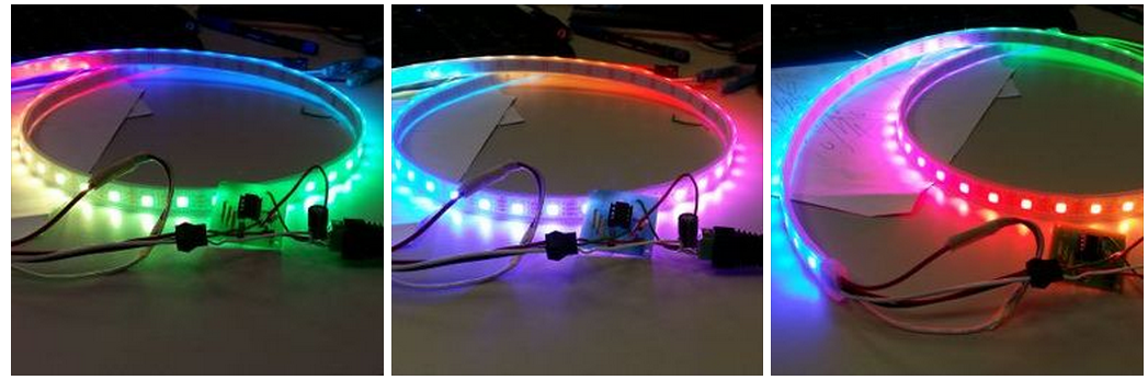
closeup
Parts needed
1x Arduino as the In System Programmer (ISP); detail guide here http://shin-ajaran.blogspot.sg/2014/01/setting-up-software-for-using-arduino.html
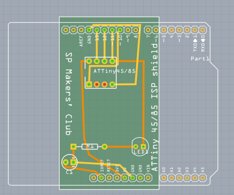
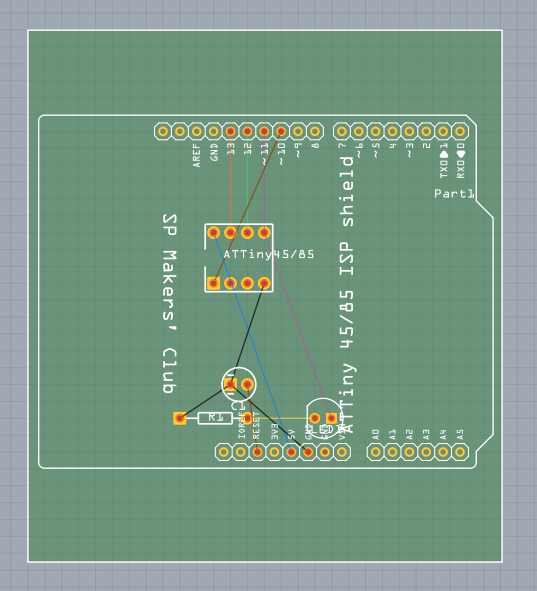
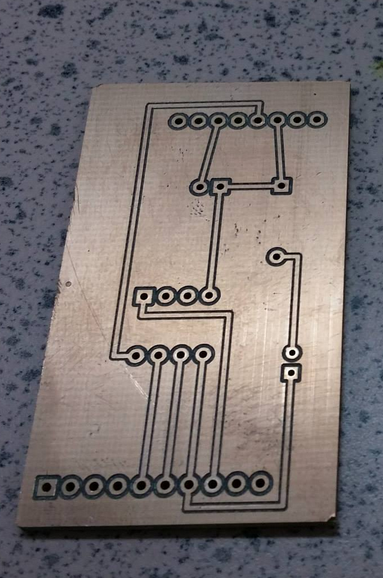
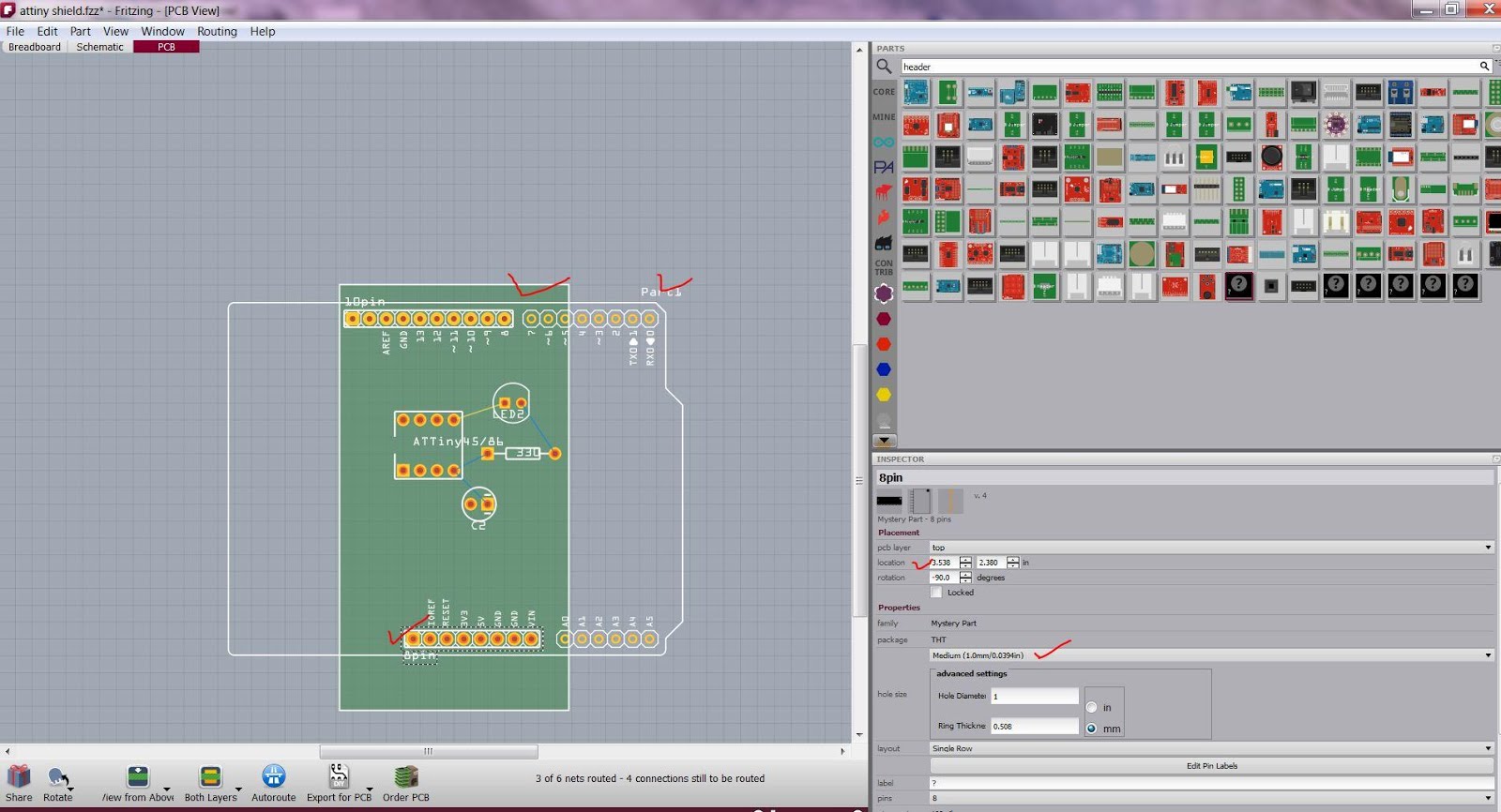
1x ATTiny85 break out board of choice; using custom MitG PCB
1x ATTiny85
1x WS2812/2811 addressable RGB LED strip (it can be neopixel from adafruit, or pseudo neopixel from middle country:aliexpress)
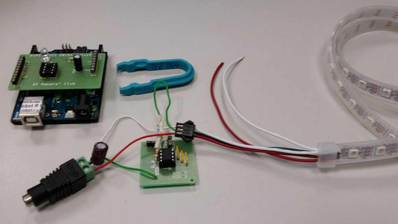
Courtesy of the techno arsenal available to SP MAKERS CLUB, all of the parts listed above are available, as per display in the image above.
Setting up the software environment
Although the RGB LED strips on hand are not Adafruit Neopixel, thanks to the Adafruit neopixel code library released on github https://github.com/adafruit/Adafruit_NeoPixel , it really saves a lot of time and effort by not re-inventing the wheel.
The “now” trend of selling a product over the Internet: In order to increase ownership from non-techines, the manufacturers will produce very detail idiot proof step by step guide. In neopixel example, the UBERGUIDE is definitely very useful. In the hands of a techie, it became some sort of cheat code, using it far from the intended purpose.
Thus, follow the UBERGUIDE (URL is in references section at the bottom of this post) closely to setup the software environment.
Setting up the hardware
Wiring is dead easy. Data pin from the addressable RGB LED strip to pin of your choice. In this case, digital pin4 of ATTiny85. NOTE: must ensure common ground by connecting ground wire of RGB LED strip to ground pin of MCU.
Programming the hardware
First, ensure all the hardware are setup accordingly to the tutorial earlier. E.g ATTiny85 on the ISP shield, ISP shield on the Arduino. USB cable is plugged in, and drivers are installed for Arduino.
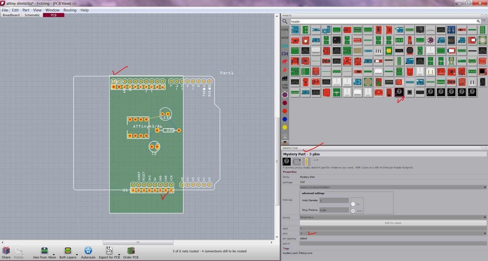
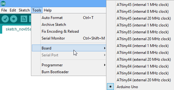
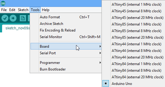
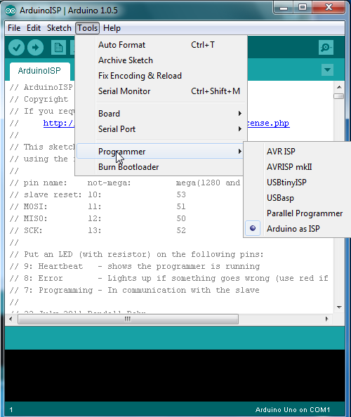
Set the “programmer” to Arduino as ISP, as depicted in the image above.
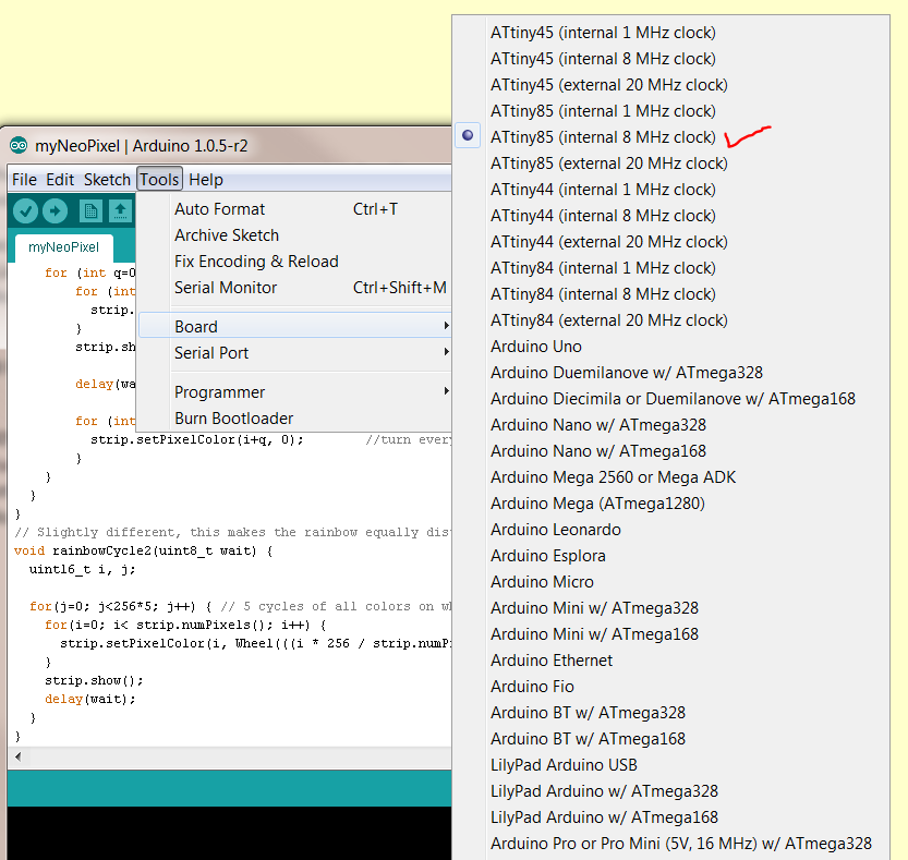
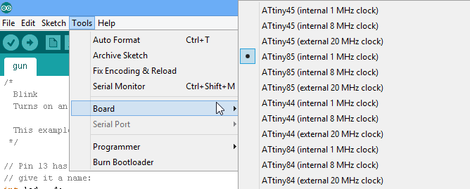
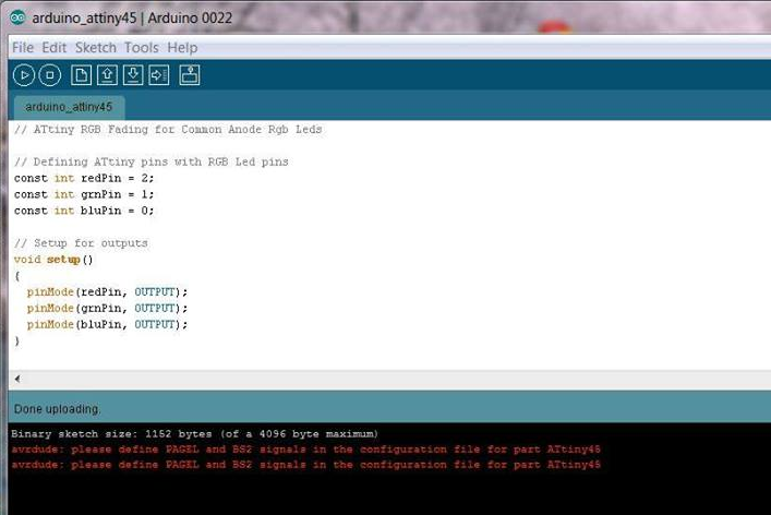
Set the “board” to ATtiny85 8MHz. Rule of thumb, choose 1MHz if low energy consumption is required, the downside, computation speed of the code will be affected. 20MHz option will not work out of the box, this option requires an external oscillator as the clock.
Set the “Serial Port” to the one detected on your computer.  
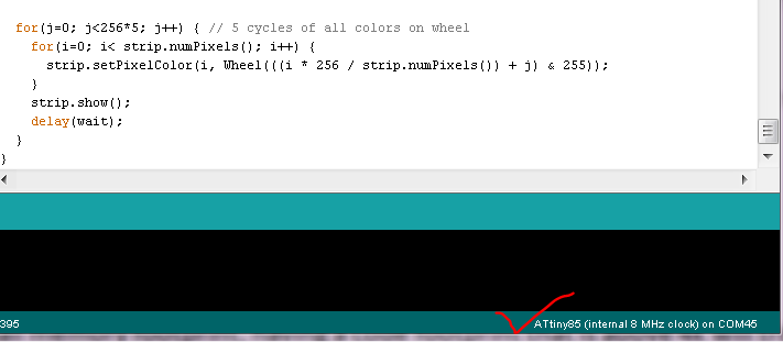
Double check the “parameters” on the lower right hand corner as depicted in the image above.
Everything seems to be prim and rosy. But we are not done yet.
If ATTiny85 is new out of the box, need to do the following step to burn the “bootloader”. Otherwise the code will be compiled, downloaded accordingly, but could not start the program upon reset.
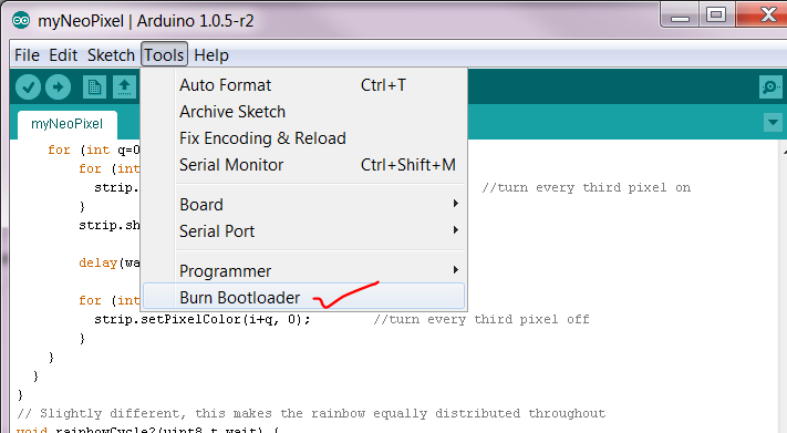
Else, the above can be skip if the ATTiny has been programmed at 8Mhz.
Source code is in public domain using the following URL
Now, click the upload button! Fingers crossed if it pleases you.
Plug in the USB power bank to test.
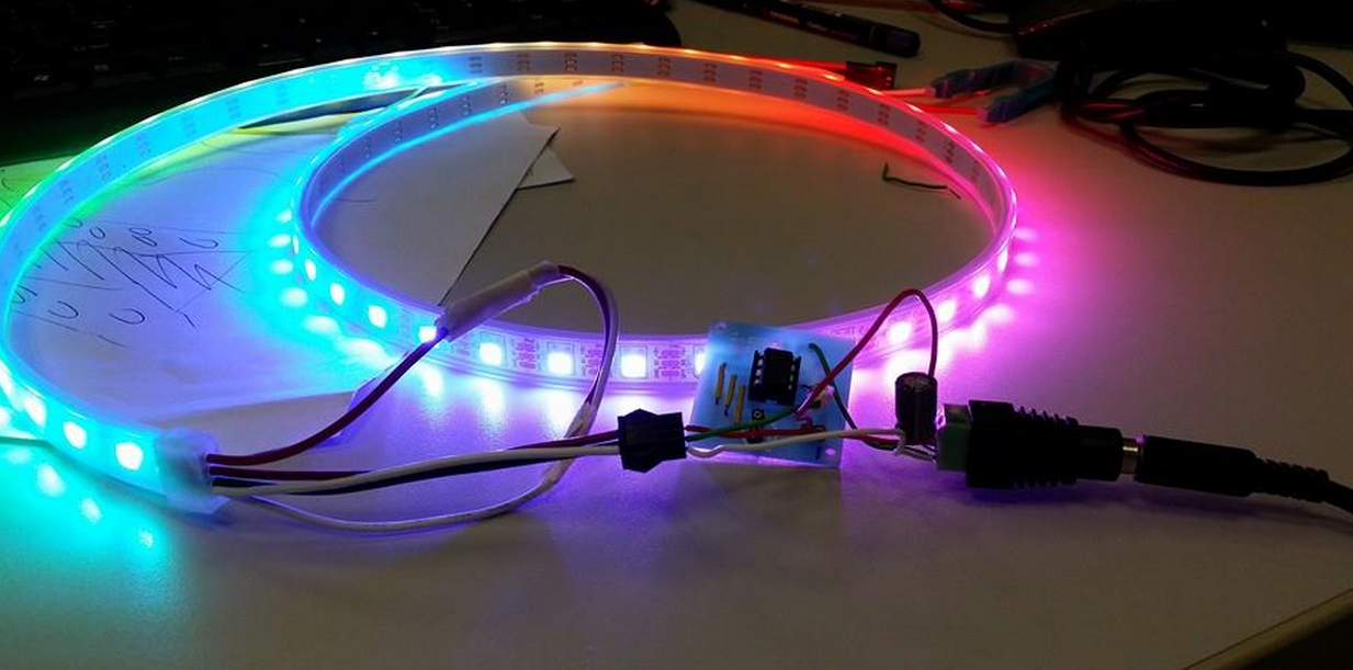
Wearable electronics = WS2812/2811 RGB LED strip+ ninjaFlex + ATTiny85 + Arduino + USB Mobile Power Bank + visibility vest
Video 


Notes:
ATTinyXX MCU has very small memory footprint; having a code footprint that is above 4k will trigger an error “relocation truncated to fit: R_AVR_13_PCREL”. Use the patch and description of the error from the following URL http://forum.arduino.cc/index.php?topic=116674.0 to fix this error
References


Monday, March 3, 2014

Project you are the ONE. a Wireless powered fiber optic side glow diffused bling

Project you are the ONE. a Wireless powered fiber optic side glow diffused bling
When I was kid, I was fascinated by the world where Tesla and Edison live in. What intrigued me most was the constant debate of AC and DC (at that time), and Tesla’s vision of having power transmitted wirelessly. No cables necessary, no copper mined unnecessarily and friendly to all humans. Wireless power transfers (inductive charging) at that time are pretty much far fetch idea. Nonetheless, the man himself went tirelessly (and possibly drove penniless) to prove his “thing”. Tesla’s destitute demise contrary to Edison’s prosperous life strikes me really hard. I nearly gave up on the dreams to study engineering; thinking I should be a business man or middle man making the in-between of deals.
While growing up, I did get my stab at making a wireless power transfer kit; reading up various recipes from various sources such as text books, “cook books” from BBS etc. , proving the materials read. At that time, I can’t even differentiate the difference between a normal copper wire and enameled wire. Both look the same to me. Without a master to guide in the field of making wireless power transfer (inductive charging) works; many failures afterwards, I came to a conclusion that probably I am better off hitched to my computer (intel 486).
Recently, while doing some read up on “Qi” the inductive power (wireless charging) standard for smartphones, suddenly I realized this might be the perfect time where the inductive charging technology has matured for end users like me to toy on the idea.
I have this idea of making novelty jewelry for the missus: wearable electronics of some sort with wireless power transfer aka inductive charging. The concept story board goes this way: At a seeming random event, I would have a little girl present her with a nicely decorated box that contains the novelty jewelry I made, with a message asking her to “follow the rabbit”. Hopefully the design of the jewelry would be very tempting such that she would put on straight away. Then a rabbit inspired character would walk pass her and hopefully, she would pick up the subtle message of following the rabbit. While following the rabbit, she will come across a few interesting characters that are staged, and the last character to appear will be me. Naturally, we would reach out to each other. Me, being the techie would have the transmitter end of inductive charging well hidden in my hand, and hook up to a ubiquitous disguised mobile power supply that supplies 12V, 1A.
Out of sudden (it is just a matter of time/distance for the EM fields to resonates between the tx loop and the rx loop), her novelty jewelry will light up and the light intensity grew greater as we are moving closer to touch! YESS! You are the one! Both of us will proclaimed. That’s the perfect time for me to take a knee, standby with a unique marriage proposal ring. 

What else? Propose to her!! this engineered piece of art definitely will work. Trust me, I am an engineer.
Oh waittttttttttttttttttttttttttttttttt…………I don’t have a missus/wife/GF yet.
This instructables assumes the following parts.
1x wireless charging kit. I got one set that is Chinese made at 13USD from aliexpress.
1x apparatus with RGB LED fading PCB of some sort, which consist of a microcontroller such as Arduino or ATTiny85, a RGB LED and a custom PCB or veroboard. A tutorial to program ATTiny85 with Arduino is available and the necessary ATTiny ISP shield can be made too.
There are many derivatives floating on the Internet. I have used my own recipe of ATTiny85 with RGB. The
step by step guide of “cooking” a PCB of your own is available here.
1x 5mm side glow fiber optic sufficient to cover the perimeter of the wearable apparatus of choice.
1x 3D printed custom made jewellery to hold the electronics, rx loop, and fiber optic. I have chosen to use a 3D printed bangle. The STL is available here. Print it twice. The two halves are snap fit. It was done in sketchup with the help from xinteng a DCPE yr1.
Step1: Assemble the RGB fading PCB, program the ATtiny 85 and mount it onto the PCB. Fiber optic cable is then inserted into a 5mm heat shrink tube. The contraption is then inserted to the 5mm RGB led.
Step2: the assembled contraption in the earlier step is then assembled with the 3D printed bangle. The fiber optic cable are is elastic, and should not be bent at sharp angles. It keep slipping out of the 5mm gap designed to hold it, so I have to resort to cable ties to hold them in place.
Step3: Test the contraption with 3V battery to test for functionality
Step4: Assemble the contraption with the RX induction coil and PCB. I have to resort to use some masking tape to keep the wires in place.
Step5: Test the contraption with TX loop connected to DC power supply. The power supply is set to 12V, 1A.
Step5: final check before turning on the DC supply. After turning on the DC supply, observe the behaviour on the EM fields w.r.t to the tx and rx loop. Note: No wireless transfer if the rx and tx loop are orthogonal to each other. The EM fields just cancel each other off.


Look! No batteries needed!

Closeup
here comes the video

Saturday, January 11, 2014

Design and fabricate a Printed Circuit Board (PCB) with Fritzing and cheat’s method to customize an Arduino shield

Design and fabricate a Printed Circuit Board (PCB) with Fritzing and cheat’s method to customize an Arduino shieldA sample screenshot of the Fritzing GUI, and a designed PCB ready to be fabricated.
Step 0: Download and install Fritzing, and familiarization with the GUI.
  1. Navigate to this URL http://fritzing.org/download/
  2. Download the Fritzing package according to your computing platform
  3. Extract the downloaded file into a folder of choice
  4. Install and launch by double clicking on the Fritzing Icon
  5. Familiarization with the Fritzing GUI. There are three tabs in the Main window panel, which offers electronics circuit in three different view. The “breadboard”, the “schematic”, and the “PCB”. Top RHS window panel offers pre-defined size of most commonly used electronics components, and also components from a myriad of vendors which include Arduino, Sparkfun, and more.
  6. The beauty of Fritzing. User can start by placing electronics components in the breadboard view or schematic view. Magically, the components will appear in the other 2 tabs that are not used. It is just a matter of preference where to start placing the electronic components.
  7. Once the electronics components are placed in the tab of choice, wiring to form the electrical connections between the electronic components can be made. The wiring connections will then be reflected in the corresponding two tabs.
  8. At the moment of writing, Fritzing does not offer simulation of circuits
Step1: Define an electronic schematic in Fritzing’s “schematics” tab
In this guide, The electronics schematic for ATtinyXX ISP shield will be assumed. While the methodology is generic, the electronics circuits should be user defined in the future use.
  1. Using the schematic above as a guide, call out the corresponding electronics components on Fritzing via the “Parts” window that is conveniently located at the top RHS panel into the “schematics” tab on Fritzing.
  2. Wiring for the connection of the components can be performed by click and hold on the point of one component, then release the click at the corresponding point of the other component. A wire will then appear.
  3. Check all wirings are done correctly and accordingly to the given schematic, in Fritzing.
  4. Now it is ready to proceed to PCB design by clicking on the PCB tab.
Step2. Design and Fabricate a PCB
In this guide, the ATtinyXX ISP shield will be assumed as an example to demonstrate the how-to of designing a PCB. A few points to note: PCB unit cost is related to two pricing components, the PCB footprint (the size of the board), and the number of layers (the copper threads layer). In other words, a smaller PCB foot print with single layer is cheaper than a bigger PCB foot print with double layer.
  1. Start PCB design by clicking on the “PCB” tab.
  2. The following screen shot best describes the designing process.
PCB resized and manual routes for double layer                       full size Arduino PCB foot print without routes
  1. In the screenshot above, the green box is the foot print of the PCB, the colour coded wiring corresponds to the wiring of electronic components made earlier. The human readable white colour text on the PCB is referred to as the “silk screen”, and it is customizable. The white colour shape outlines the physical perimeter of an Arduino and the relative position of the two rows of header pins. Using this predefined template from Fritzing, the to-be-created Arduino shield will fit the Arduino in a snug fit.
  2. Next is to add the routes. Routes on the PCB refer to the wiring of copper threads that connects electronic components. There are two camps or school of thoughts when it comes to placing routes on a PCB. First is the “auto-route” that requires minimal human intervention. Lastly the manual route that requires a lot of human attention. Placing of routes requires both functionality, and aesthetics. The routes must not be not too close to each other, and not overlapping to each other causing a short circuit.
  3. At any time when designing the routes in Fritzing, routes can be deleted or undo.
  4. Auto route by pressing the “Auto Route” button in Fritzing
  5. Manual route by clicking on the individual wires from one end to the other end.
  6. When route design is finalized, perform a design rule check by pressing Ctrl+Shift+D. Fritzing will recommend if the PCB design is ready to be fabricated.
  7. Export the PCB design into gerber files (RS-274X) by clicking on the “Export for PCB” button and send it to your local vendor to fabricate.
  8. The generated gerber files can be view using open source software such as gerbv.
Step3. Design a custom foot print PCB Arduino Shield using cheat’s method
From the previous step, it is not difficult to notice something is amiss from the foot print of the PCB relatively to the size of the electronic schematic, and also the number of holes need to be drilled. In this guide, a non-conventional method will be used to generate custom small foot print PCB for Arduino that fits like a glove. The three diagrams below best describe the process of digital fabrication of a custom foot print Arduino shield PCB from software to physical prototype. The diagram on the left is the final design of the custom foot print PCB with this cheat’s method. The gerber file from the PCB design is then used to produce a prototype with the PCB milling machine, the sample is the center diagram. Lastly the diagram on the right describes the operational custom foot print PCB Arduino shield.   
  1. In this guide, the same electronic components as assumed as per the previous step.
  2. The wiring between Arduino and the rest of the components are not connected in the “schematic” tab.
  3. From the “Parts” window panel, add the customizable “mystery part – 3 pin” into the PCB tab. This “mystery part – 3 pin” can be customized accordingly to the number of pins required by the design of the PCB. In this example, two rows of custom header of 10 pins and 8pins each are added. The following diagram describes the use of “mystery part”.
  4. Using the unconnected Arduino as a reference template, overlap with the 8pin and 10pin “mystery part” correspondingly. This shall give the relative position of the pin headers on the custom foot print PCB to the actual Arduino.   The
  5. Connect the routes as per the previous step from the electronic components to the “mystery parts” as if it is the Arduino. Once completed, delete the reference Arduino.
  6. Now a custom foot print PCB as Arduino shield is ready. The net effect is the savings on the unit cost and time taken to produce this shield commercially.
References
  1. Fritzing help and tutorials http://fritzing.org/learning/
  2. Gerbv, a gerber file viewer. http://sourceforge.net/projects/gerbv/

Saturday, January 4, 2014

Setting up the software for using Arduino as the In System Programmer (ISP) to download program onto ATtiny85

Setting up the software for using Arduino as the In System Programmer (ISP) to download program onto ATtiny85

Step0: Install ATTiny Cores
NOTE: This Tutorial assumes Arduino v1.0.x and above has been installed on the computer.
Go to this URL https://github.com/damellis/ATtiny/archive/master.zip and download this file: master.zip  
Extract this file and copy the entire folder to the “hardware” folder of your Arduino installation directory. Note: The following screen is mine and might differ from yours.
Restart the Arduino IDE programming environment. 
Verify the new cores (ATtinyXX series) loaded in Arduino IDE.
Note that there are also other core files for a variety of ATtiny chips loaded e.g ATting85. This page is a good starting point for interfacing with a wide range of the ATtiny or ATtiny85 using the Arduino.

Click on Tools , Board to verify the variety of ATtiny chips.

Programming the ATtinyXX chip with Arduino as the ISP
Note: This is a 1 + N step. Step 1 requires setting up the Arduino as the ISP for the first time progamming of an ATtiny. Step N has to be repeated every time to program an ATtiny. The ATtiny chip has to be placed on the ATtinyXX ISP shield, and then connected to the Arduino. The program will then be downloaded to ATtiny instead of Arduino.


Step1: Setting up Arduino as the ISP
  1. Connect usb cable to Arduino
  2. Go to Tools->Board and make sure Arduino Uno is selected.
  3. Make sure that the correct serial port is selected.
  4. Go to Tools->Programmer -> Arduino as ISP
  5. Go to Examples -> ArduinoISP
  6. Click  to upload the ISP program to the Arduino
  7. Now your arduino is ready to be used to program it's poor cousin, the ATtiny85.


Step N part1: ATtinyXX chip is inserted into ATtinyXX ISP shield; shield is then connected to the Arduino.
  1. Confirm USB cable is unplugged from Arduino when inserting the ISP shield
  2. Align ATtiny85 DIP8 package chip to ATtiny85 ISP shield
  3. Insert ATtiny85 chip firmly onto the ISP shield
  4. Align ISP shield to Arduino
  5. Insert ISP shield firmly onto Arduino
Question: What is the model of the ATtiny chip in the picture above?
Note: ATtiny45/85-PU is 20MHz (with external clock). refer to the datasheet at References.

Click here for highres picture
https://www.dropbox.com/sc/bo8yblnevzrf1vu/KrTsbTAOBU


Step N part 2: Download your programming code to ATtiny85
  1. Confirm chip, shield, and Arduino is plugged into USB.
  2. Select the corresponding code of choice (e.g *.ino) file to be programmed onto the ATtiny85 chip by clicking File-> Open.
  3. Go to Tools -> Board and make sure this time you choose ATtiny85(internal 1 MHz clock)
  4. Click  to upload the program.
  5. Upon success, you should see the message below. Ignore the warnings. The ATtiny chip has been programmed.
  6. Observe the output of the operational ATtiny85 programmed with the code specified.


NOTE: by default ATtiny85 comes with 1MHz clock internal. This clock can be modified to 8MHz internal by the selecting option "Burn Bootloader" while selecting the option "ATtiny85(internal 8MHz clock)". Subsequent programming of ATtiny85 need to choose the board option "ATtiny85(internal 8MHz clock)"
References


Addendum: Old version of Arduino, e.g Arduino 0022


New ATtiny cores eg ATtiny85 on Arduino 0022


Select ATtiny45-20PU as the board (requires external oscilator to function at 20MHz)


Download RGB LED code to ATtiny45