Design and fabricate a Printed Circuit Board (PCB) with Fritzing and cheat’s method to customize an Arduino shield A sample screenshot of the Fritzing GUI, and a designed PCB ready to be fabricated.
A sample screenshot of the Fritzing GUI, and a designed PCB ready to be fabricated.
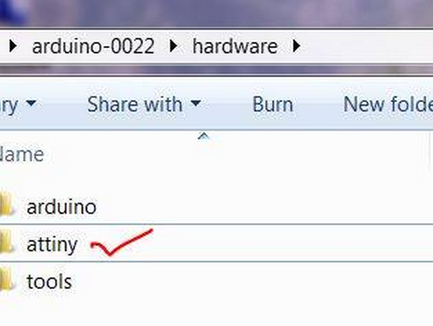
Step 0: Download and install Fritzing, and familiarization with the GUI.
- Navigate to this URL http://fritzing.org/download/
- Download the Fritzing package according to your computing platform
- Extract the downloaded file into a folder of choice
- Install and launch by double clicking on the Fritzing Icon
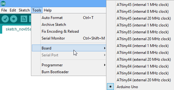
- Familiarization with the Fritzing GUI. There are three tabs in the Main window panel, which offers electronics circuit in three different view. The “breadboard”, the “schematic”, and the “PCB”. Top RHS window panel offers pre-defined size of most commonly used electronics components, and also components from a myriad of vendors which include Arduino, Sparkfun, and more.
- The beauty of Fritzing. User can start by placing electronics components in the breadboard view or schematic view. Magically, the components will appear in the other 2 tabs that are not used. It is just a matter of preference where to start placing the electronic components.
- Once the electronics components are placed in the tab of choice, wiring to form the electrical connections between the electronic components can be made. The wiring connections will then be reflected in the corresponding two tabs.
- At the moment of writing, Fritzing does not offer simulation of circuits
Step1: Define an electronic schematic in Fritzing’s “schematics” tab
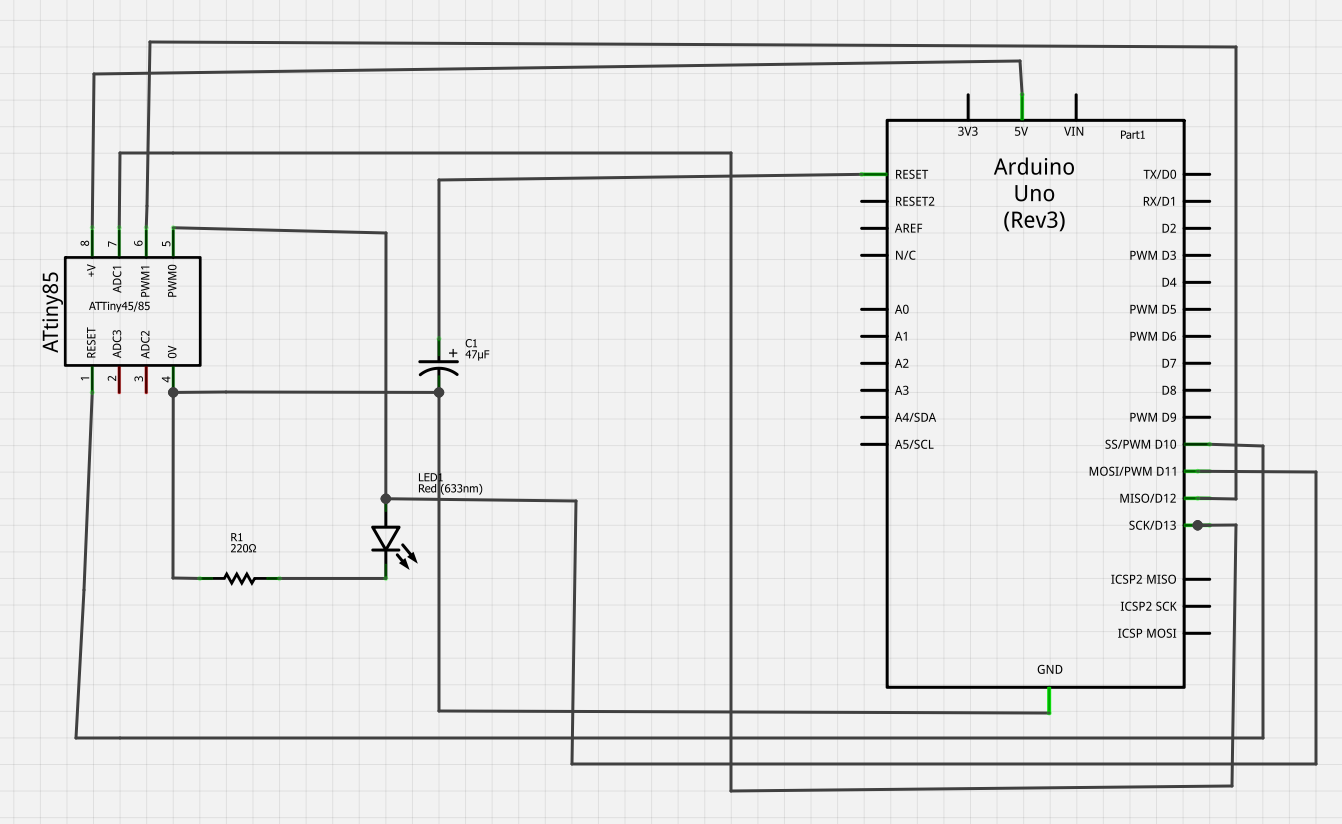
In this guide, The electronics schematic for ATtinyXX ISP shield will be assumed. While the methodology is generic, the electronics circuits should be user defined in the future use.
In this guide, The electronics schematic for ATtinyXX ISP shield will be assumed. While the methodology is generic, the electronics circuits should be user defined in the future use.
- Using the schematic above as a guide, call out the corresponding electronics components on Fritzing via the “Parts” window that is conveniently located at the top RHS panel into the “schematics” tab on Fritzing.
- Wiring for the connection of the components can be performed by click and hold on the point of one component, then release the click at the corresponding point of the other component. A wire will then appear.
- Check all wirings are done correctly and accordingly to the given schematic, in Fritzing.
- Now it is ready to proceed to PCB design by clicking on the PCB tab.
Step2. Design and Fabricate a PCB
In this guide, the ATtinyXX ISP shield will be assumed as an example to demonstrate the how-to of designing a PCB. A few points to note: PCB unit cost is related to two pricing components, the PCB footprint (the size of the board), and the number of layers (the copper threads layer). In other words, a smaller PCB foot print with single layer is cheaper than a bigger PCB foot print with double layer.
In this guide, the ATtinyXX ISP shield will be assumed as an example to demonstrate the how-to of designing a PCB. A few points to note: PCB unit cost is related to two pricing components, the PCB footprint (the size of the board), and the number of layers (the copper threads layer). In other words, a smaller PCB foot print with single layer is cheaper than a bigger PCB foot print with double layer.
- Start PCB design by clicking on the “PCB” tab.
- The following screen shot best describes the designing process.
PCB resized and manual routes for double layer full size Arduino PCB foot print without routes
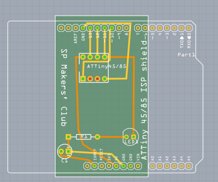
- In the screenshot above, the green box is the foot print of the PCB, the colour coded wiring corresponds to the wiring of electronic components made earlier. The human readable white colour text on the PCB is referred to as the “silk screen”, and it is customizable. The white colour shape outlines the physical perimeter of an Arduino and the relative position of the two rows of header pins. Using this predefined template from Fritzing, the to-be-created Arduino shield will fit the Arduino in a snug fit.
- Next is to add the routes. Routes on the PCB refer to the wiring of copper threads that connects electronic components. There are two camps or school of thoughts when it comes to placing routes on a PCB. First is the “auto-route” that requires minimal human intervention. Lastly the manual route that requires a lot of human attention. Placing of routes requires both functionality, and aesthetics. The routes must not be not too close to each other, and not overlapping to each other causing a short circuit.
- At any time when designing the routes in Fritzing, routes can be deleted or undo.
- Auto route by pressing the “Auto Route” button in Fritzing
- Manual route by clicking on the individual wires from one end to the other end.
- When route design is finalized, perform a design rule check by pressing Ctrl+Shift+D. Fritzing will recommend if the PCB design is ready to be fabricated.
- Export the PCB design into gerber files (RS-274X) by clicking on the “Export for PCB” button and send it to your local vendor to fabricate.
- The generated gerber files can be view using open source software such as gerbv.
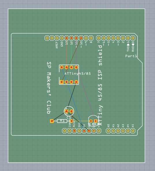
Step3. Design a custom foot print PCB Arduino Shield using cheat’s method
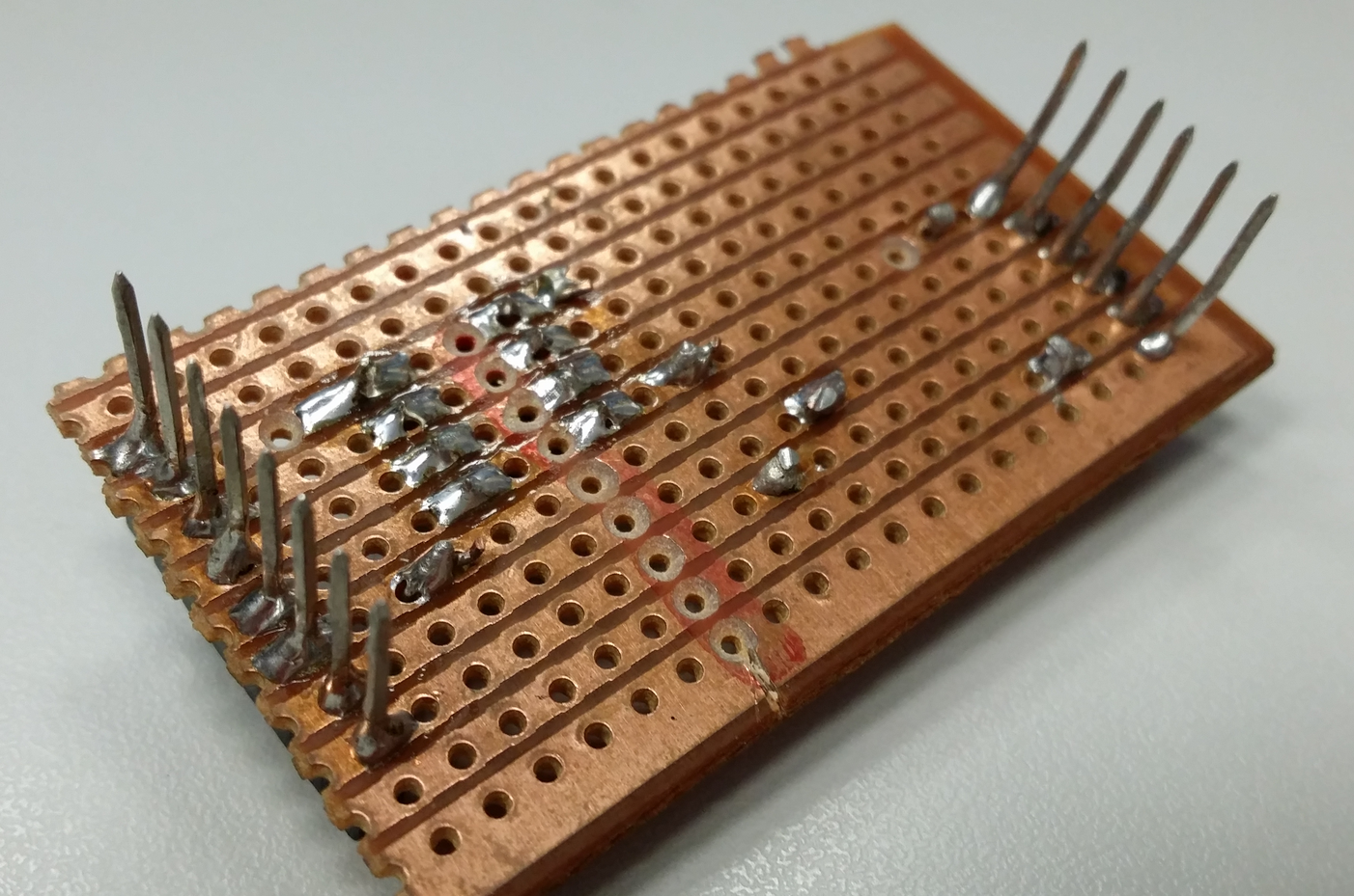
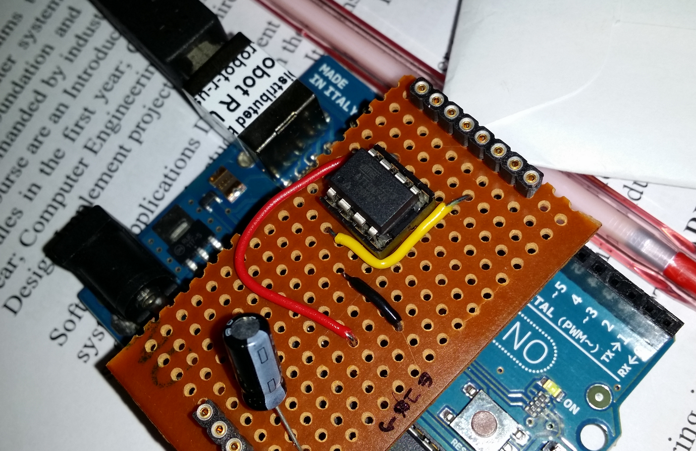
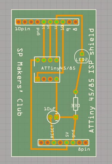
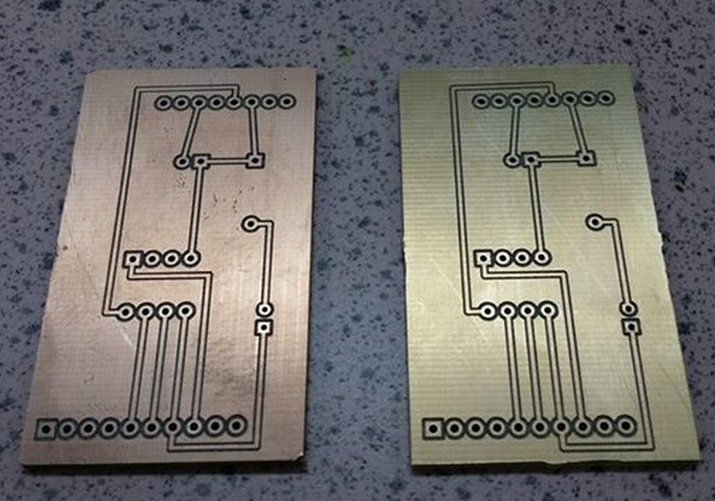
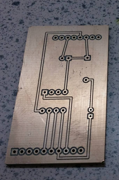
From the previous step, it is not difficult to notice something is amiss from the foot print of the PCB relatively to the size of the electronic schematic, and also the number of holes need to be drilled. In this guide, a non-conventional method will be used to generate custom small foot print PCB for Arduino that fits like a glove. The three diagrams below best describe the process of digital fabrication of a custom foot print Arduino shield PCB from software to physical prototype. The diagram on the left is the final design of the custom foot print PCB with this cheat’s method. The gerber file from the PCB design is then used to produce a prototype with the PCB milling machine, the sample is the center diagram. Lastly the diagram on the right describes the operational custom foot print PCB Arduino shield. 

- In this guide, the same electronic components as assumed as per the previous step.
- The wiring between Arduino and the rest of the components are not connected in the “schematic” tab.
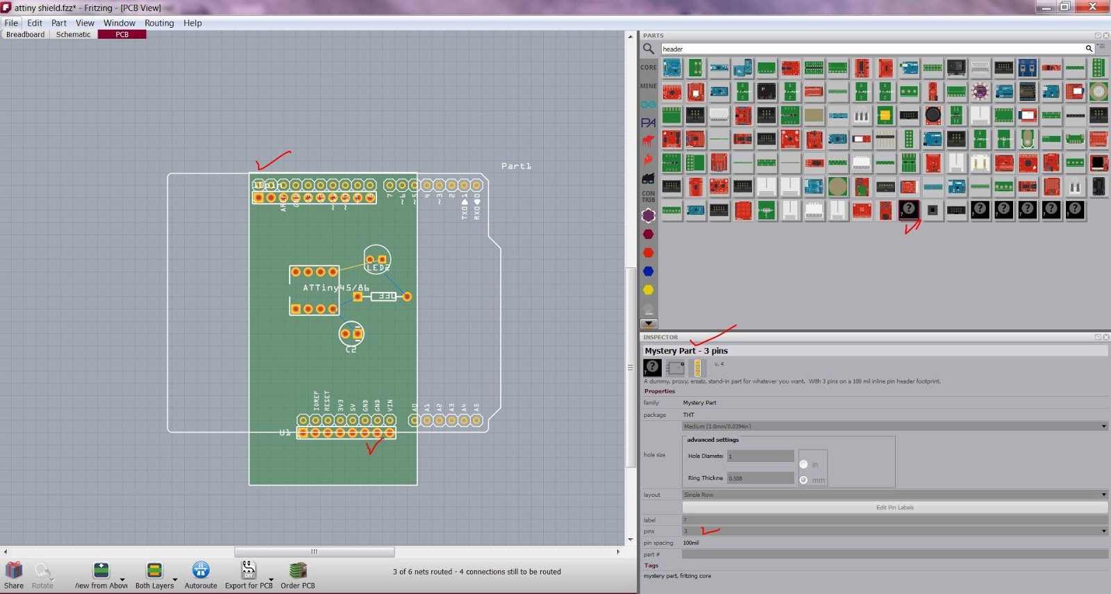
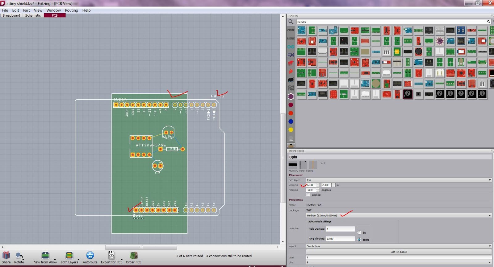
- From the “Parts” window panel, add the customizable “mystery part – 3 pin” into the PCB tab. This “mystery part – 3 pin” can be customized accordingly to the number of pins required by the design of the PCB. In this example, two rows of custom header of 10 pins and 8pins each are added. The following diagram describes the use of “mystery part”.
- Using the unconnected Arduino as a reference template, overlap with the 8pin and 10pin “mystery part” correspondingly. This shall give the relative position of the pin headers on the custom foot print PCB to the actual Arduino. The
- Connect the routes as per the previous step from the electronic components to the “mystery parts” as if it is the Arduino. Once completed, delete the reference Arduino.
- Now a custom foot print PCB as Arduino shield is ready. The net effect is the savings on the unit cost and time taken to produce this shield commercially.
References
- Fritzing help and tutorials http://fritzing.org/learning/
- ATTiny XX ISP hardware user guide http://shin-ajaran.blogspot.sg/2014/01/setting-up-hardware-for-using-arduino.html
- Gerbv, a gerber file viewer. http://sourceforge.net/projects/gerbv/